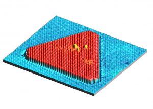
The most important drawback of graphene, this “best-for-all” material, for application in electronics and optoelectronics is the abscence of an electronic gap. This can be induced by scaling down the material to dimensions where electrons can be quantized. Indeed, nanometer size graphene structures exhibit quantization gaps that are comparable to that of the inherent gap of semiconductors used in actual electronic devices. this is also crucial for the optical response of the material, since it shifts optical and plasmonic resonances from the infrared towards the visible regime demanded by telecomunication. The presence of edges might also result in the emergence of novel phenomena, such as the existence of dissipationless one dimensional magnetic states.
All the above properties depend on the size and morphology of the nanostructure, but at this scale they are also particularly sensitive to the atomic structure, both of thet bulk and of the edges. Magnetic edge states will exist at zig zag edges, but not at armchair edges. On the other hand, the latter are more efficient on inducing quantization band gaps. It is fundamental, hence, to control the synthesis of graphene nanostructures at the atomic scale.
Our group has developed a bottom-up method based on chemical vapour deposition that allows to synthesize graphene nanostructures with control on the overall morphology, and crystal structure of both the bulk and the edges. By tuning the growth parameters, we are able to control the topological defects of the bulk, induce edge reconstructions, and shape illdefined clusters into shape-selected triangular and hexagonal nanostructures.
Reference
